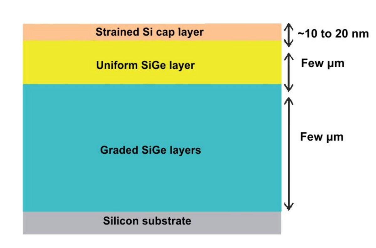

Mechanical strain directly affects the frequency positions of the Raman modes and can lift their degeneracy. Typically, it is possible to observe and detect strain by analyzing the shift in the band position, but it can also affect the band shape and induce broadening and deformation peaks.
Raman spectroscopy is one of the most popular tools for investigating the basic properties of semiconductors. It is particularly efficient in establishing the characteristics of microelectronic devices because the performance of SiGe based devices highly depends on the knowledge of the composition, Ge content and the strain of the layers. Indeed, the ability to measure alloy composition and strain in semiconductor structures is essential for the calibration of growth processes and control of the electrical and optical behavior of these materials.
The first requirement for the study of mechanical stress with Raman spectroscopy is that the investigated material exhibits Raman active modes, ie that there is a well defined Raman band in the spectrum. These include materials such as diamonds, silicon, SiGe, InGaAs, GaAs, GaN, to name a few. Mechanical strain directly affects the frequency positions of the Raman modes and can lift their degeneracy.
Typically, it is possible to observe and detect strain by analyzing the shift in the band position, but it can also affect the band shape and induce broadening and deformation peaks. These effects depend upon the material characteristics and on the stress and strain geometry. In this study, we focus on the choice of the laser excitation and measurement conditions. Results obtained in the visible and in the UV range are presented.
Raman Spectroscope - Automated Imaging Microscope
Confocal Raman Microscope
MicroRaman Spectrometer - Confocal Raman Microscope
Confocal Raman & High-Resolution Spectrometer
Do you have any questions or requests? Use this form to contact our specialists.
