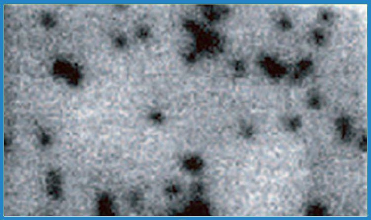

The crystal may seem to be uniform in the SEM image, but the dark spot such as the threading dislocation can be observed when measuring the CL intensity image at the wavelength (362nm) which corresponds to the band edge emission.
The threading dislocation occurs easily in GaN crystal grown on sapphire substrates. It is said that this is caused by the large lattice mismatch of sapphire and GaN.
The crystal may seem to be uniform in the SEM image, but the dark spot such as the threading dislocation can be observed when measuring the CL intensity image at the wavelength (362nm) which corresponds to the band edge emission.
The defect density such as the threading dislocation can be evaluated from the intensity image obtained by CL measurement.
Raman Photoluminescence & Cathodoluminescence
Versatile Hyperspectral Cathodoluminescence
Compact Hyperspectral Cathodoluminescence
Fast Imaging Cathodoluminescence
Cathodoluminescence Solutions for Electron Microscopy
Do you have any questions or requests? Use this form to contact our specialists.
