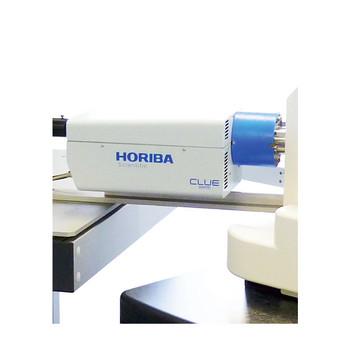
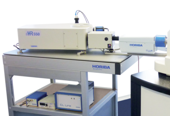
Cathodoluminescence measurement system HORIBA CLUE series
- Can be added to existing electron microscopes
- Compatible with measurements at ultraviolet to near-infrared wavelengths (200 to 2,100 nm)
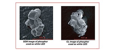
- SEM integrated high range CL imaging device (Imaging CL) can also be proposed.
Cathodoluminescence - CLUE Series
Cathodoluminescence Solutions for Electron Microscopy
F-CLUE
Compact Hyperspectral Cathodoluminescence
H-CLUE
Versatile Hyperspectral Cathodoluminescence
R-CLUE
Raman Photoluminescence & Cathodoluminescence
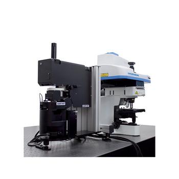
AFM (atomic force microscope) Raman XploRA Nano
- Acquire physical information by AFM and chemical information by Raman simultaneously
- Stress distribution analysis on the outermost surface on the order of nm is possible.
XploRA Nano
AFM-Raman for Physical and Chemical imaging
