Latest issue of HORIBA Technical News Letter “e-Readout”
Abstract Magnetism is mysterious thing. Despite magnetic fields being everywhere, from the one generated by the Earth and surrounding us, to the tiny ones within the molecules of our body, they remain invisible to the human eye, hidden to our senses. Over the years, however, the development of sensing techniques allowing the observation, understanding and control of magnetism have led to a series of revolutions from the first compass used for navigation to the MRI scanner used every day in our hospitals. Yet, classical technologies are now reaching their limits.


Mathieu Munsch
CEO, Qnami AG
Switzerland
► Click Here to original paper (PDF file)
Measuring minute magnetic fields with NV centers in diamond
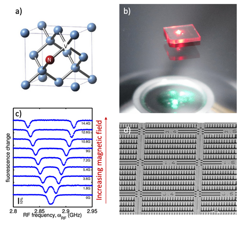
Quantum sensors, which leverage the extreme sensitivity of quantum systems to their environment, offer radically new performance. Their ability to measure weak signals down to the single molecule level unlock new perspectives in early stage diagnostics, in the development of novel energy-efficient electronics circuits as well as in security. Among the existing technological platforms, quantum sensors based on so-called NV centers (or nitrogen-vacancy centers) in diamond stand out. Diamond is a wonder material on many fronts. It is robust, inert and bio-compatible, allowing for nonperturbing measurement in the most challenging environments. Ultra-high quality diamond is produced industrially while microfabrication processes allow to functionalize and cut the diamond with the same techniques as in the silicon industry. Diamond is also the perfect material for a quantum sensor. The diamonds used for quantum applications contain defects in their crystal lattice, where two carbon atoms have been swapped for a nitrogen atom and a vacant site immediately alongside. These defects are known as nitrogen-vacancy centers (NV centers) and can also occur in natural diamonds, where they impart a reddish color to the precious stones (see Figure 2 a and b). By trapping one extra electron, NV centers can be turned into a microscopic compass - a spin with atomic size. Through precise manipulation and measurement of the state of this NV spin, one can measure the smallest changes in the surrounding magnetic field, a technique called NV magnetometry.

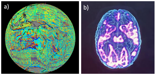
Figure. 1: Measuring the invisible.
a) Magnetic fields at the surface of the Earth (Credits Earth Bytes).
b) Brain activity revealed by magnetic resonance imaging (MRI)
NV magnetometry: how it works
NV magnetometry relies on the interaction between the NV center and the surrounding magnetic field. The presence of a magnetic field manifests by a modification of the energies of the NV center spin states. Typical data from an NV magnetometer is shown in Figure 2c. The effect of the magnetic field is readily seen in the modification of the NV center microwave excitation spectrum. A crucial advantage of NV magnetometry comes from the well understood behavior of the NV center spin transition frequencies, which provide unambiguous information about the strength and the direction of the magnetic field. This ability to provide self-calibrated, quantitative data, combined with a very high reproducibility (each and every NV center is the same) are key intrinsic features of NV-based quantum sensors. But the principal advantage of quantum sensors lies in their sensitivity to very small signals. Specifically, the sensitivity of an NV magnetometer to DC magnetic fields depends on 1) the density of NV centers within the diamond chip, 2) the quantum coherence of said NVs, and 3) the efficiency of the optical read-out. Theoretical sensitivities range from one micro Tesla per second integration time for single NV centers (used in high spatial resolution applications) down to a few pico Tesla for dense NV ensembles. In practice though, reaching this level of performance can prove challenging. Indeed, the quantum coherence is a fragile property which is easily damaged when increasing the NV center density or when engineering the diamond crystal itself. Using micro-fabrication techniques inspired by the silicon industry Qnami has developed proprietary processes to produce advanced NV diamond chips which leaves their quantum properties intact (see Figure 2 d).

Figure. 2: NV Magnetometry.
a) Nitrogen-vacancy center in the diamond crystal.
b) A diamond crystal (top) emits red light upon illumination with a green laser (bottom),
the signature of NV centers in the crystal (Credits Hatano-Iwasaki Lab, Tokyo Institute of Technology)
c) ODMR spectra as a function of the external magnetic field (1G = 1 Gauss = 0.01 mT).
d) NV diamond by Quami. The surface has been engineered into an array of scanning probes in a
way to maximize light extraction while preserving the quantum coherence of the embedded
NV centers. Both aspects contribute to a high sensitivity.
The ability to measure small magnetic fields is key for a large variety of applications going from navigation to diagnostics, to electronics. For instance, NV sensors are being developed for navigation, where they allow for a reliable positioning on the surface of the Earth, similar to the GPS, but with the advantage of being free of any requirement of communication with an external device (like a satellite). Such navigation systems are not only of great importance for defense, but could also apply in the context of autonomous vehicles, as a safety back up for the
cases of failing GPS connections. In healthcare, NV sensors are being developed to enable the detection of ultra-low concentrations of target biomarkers, removing the need for large test samples and offering new perspective in early diagnostics. Finally, in electronics NV sensors can be applied in quality control of integrated circuits. There, the measurement of magnetic field patterns allows tracing electrical currents in a microchip and potentially identifying manufacturing defects or deviations from the intended design.
The requirements on the NV sensors may vary depending on their use but such magnetometers always comprises the following core components:
• an NV diamond chip,
• an excitation source (typically a green laser diode),
• a high sensitivity optical detector (typically a single photon counter),
• a tunable microwave source (2.5-3.5GHz range).
Depending on the application, these elements can either be integrated around the diamond chip to make a compact sensor or left as separate components of a larger system. While the former option is well suited for the mobile measurement of weak, diffuse signals, the latter is favored for the study of small signals with microscopic origin. In practice – and this represents an additional key feature of NV sensors – the atomic size of the NV center offers the possibility to produce magnetic maps with nanometer spatial resolution. But such applications faces a further challenge: the necessity to bring the NV sensors in extremely close proximity to the magnetic source.
Nanoscale NV magnetometry
In a similar way to classical magnetic field sensors, which are moved around the Earth by satellites and airplanes in order to map the Earth’s magnetic field (see Figure 1), quantum sensors can be precisely maneuvered over tiny magnetic structures to map and visualize magnetic properties with nanoscale spatial resolution. This is achieved through a technique called Scanning NV Magnetometry.
Scanning NV magnetometry relies on the use of a sharp, microscopic NV diamond tip, which is scanned at a controlled distance of just a few nanometer from a sample. As the tip flies over the surface, both the sample’s topography and its magnetic textures are recorded, producing unique images in nanoscale resolution.
In order to provide the best spatial resolution, the NV center is brought in very close proximity to the tip apex. Indeed, while the tip’s radius of curvature determines the lateral resolution for the topography image, the distance between the NV center and the sample surface determines the lateral resolution for the magnetic image. The patented Quantilever MX design from Qnami, brings the NV center as close as ten nanometers away from the tip apex, offering the highest spatial resolution amongst all existing magnetometers. Remarkably, the Quantilever MX design simultaneously ensures an efficient routing of the NV optical signal, thereby maximizing sensitivity and overall performance.

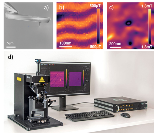
Figure. 3: Scanning NV Magnetometry.
a) Image of a Quantilever MX recorded with a scanning electron microscope.
b) and
c) Images of the magnetic textures at the surface of antiferromagnets BiFeO3 and Mn3GaN.
The data is obtained using the Qnami ProteusQ (d), the first commercial scanning
NV magnetometer, developed by Qnami in partnership with Horiba Scientific.
Figure 3 illustrates the outstanding performance of scanning NV magnetometry. The images reveal the magnetic textures at the surface of a very special class of magnets known as antiferromagnets, whose peculiar properties have generated strong interest for the next generation of low-power electronic devices. Yet, despite the craze around such materials, the direct observation of their magnetic properties has remained a challenge, possible only with large scale instruments such as synchrotron light sources. Here, the data have been recorded using the Qnami ProteusQ, a complete quantum microscope and the first commercially available Scanning NV Magnetometer.
This table-top system was developed by Qnami in partnership with Horiba Scientific. Compared to the previously available approach for nanoscale studies of antiferromagnets, which was based on synchrotron light sources, the Qnami ProteusQ offers simple operation, fast sample turnaround times, easy integration of Quantilevers as well as a leap in precision, through a 10x improvement in spatial resolution.
These features are key for the study of a new generation of advanced materials for spintronics applications, including ultra-thin ferromagnets, antiferromagnets, multiferroics, 2D materials and more. In addition, beyond the fundamental study of such materials, the on-going development of MRAM technology is shining light on the needs of the semiconductor industry to access new metrology tools and standards. While magnetic properties of materials have been largely ignored for electronic devices, the electronics of tomorrow is taking a new spin, and NV magnetometry will make decisive contribution.
DISCLAIMER
The content of this document is copyrighted by Qnami AG. Qnami AG makes no warranties with respect to the accuracy or completeness of the content in this document and reserves the right to make changes to the specification at any time without notice. All trademarks are the property of the company Qnami AG.
Quami AG 2017-2021
Product & Exhibition information, Contact information
- ProteusQ is a high performance, compact, stable and easy to use Scanning NV Magnetomer.
It enables non-invasive measurement of magnetic fields with unprecedented sensitivity and nanoscale spatial resolution.
- ProteusQ is the first commercial quantum microscope, and the only scanning NV magnetometer produced under exclusive license to patents from Harvard.
It is based on Qnami proprietary quantum sensing technology and HORIBA’s deep expertise in optical coupling to AFM (Atomic Force Microscopy).
Contact information:
Dr Marc CHAIGNEAU, HFR, marc.chaigneau@horiba.com
For more information about ProteusQ, please visit: HORIBA
Upcoming Event (Plans to exhibit):
Sol-SkyMag 2021 | 21 - 24 June 2021 (Intl. conference on magnetism & spintronics) Scientific talk by Hai Zhong (Qnami)
Upcoming e-Readout issues: Topics on water quality monitoring
e-Readout Editorial Office:
Research & Development Division, HORIBA, Ltd.
2, Miyanohigashi-cho, Kisshoin, Minami-ku, Kyoto 601-8510, Japan
E-mail : readout(at)horiba.co.jp
