Latest issue of HORIBA Technical News Letter “e-Readout”
Abstract This article reports on nano-characterization of 2D transition metal dichalcogenides (TMDCs) materials which are considered of very high potential semiconductors for future nanosized electronic and optoelectronic devices. Atomic force microscopy (AFM) giving access to the critical topographic and electronic properties at the nanoscale is coupled to photoluminescence (PL) and Raman spectroscopies by means of plasmon enhancement to yield correlated electrical and chemical information down to the nanoscale.
Click Here to original paper (PDF file)
Introduction
2D materials are defined as crystalline materials consisting of a single unit cell layer of that material. Among the large number of potentially stable 2D materials (more than 700), graphene and the family of transition metal dichalcogenides (TMDCs) are under thorough study as candidates for tomorrow‘s nanoelectronics building blocks. Monolayer TMDCs are tunable band gap semiconductors and complement zero gap graphene. A myriad of nanoelectronics applications are foreseen, ranging from transistors to photodetectors as well as in the energy field (nanogenerators, green electronics, electrocatalytic hydrogen generation and energy storage). Many challenges remain before the promise of 2D materials is realized in the form of practical nano-devices, e.g.: (i) understanding growth mechanism of these crystals, to be able to fabricate defect-free large area film, (ii) controlling transfer processes from growth substrates to another surface substrates, (iii) controlling their vertical or lateral integration. An information-rich, nanoscalecharacterization technique is required to qualify these materials and assist in the deployment of 2D material-based applications. On one hand, Raman and photoluminescence spectroscopies are the techniques of choice to characterize monolayer crystalline materials in terms of electronic behavior (band gap, carrier concentration) and structural quality (defect location and density). On the other hand, atomic force microscopy (AFM) has been a key enabling tool for the development of nanomaterials producing not only topographic images with atomic resolution but also probing the physical (electrical, magnetic, mechanical…) properties of surfaces. But both Raman/PL and AFM have their limits: (i) because conventional Raman is a far-field optical technique (the spot size is diffraction-limited), its applications are restricted to the micro- and macro-worlds, (ii) AFM delivers only physical information images. Plasmon-enhanced optical spectroscopies (TEPL: Tip-Enhanced Photoluminescence, TERS: Tip-Enhanced Raman Spectroscopy) bridge the gap to NanoRaman and NanoPL offering optical, nanometric spatial resolution. Furthermore, these new spectroscopic techniques combined with the AFM modes for multi-parameter analysis of 2D materials [1, 5] offer the best of both worlds and open up new possibilities for the characterization of chemical, optoelectronic, topographic and electronic properties of 2D materials.
Experimental
Plasmon-enhanced optical spectroscopies (TEPL and TERS) are based on the amplification of signal from the nano-region under the noble metal coated AFM tip on which the Raman excitation laser is focused.
Results reported here have been obtained from one of our HORIBA AFM-Raman systems: XploRA Nano or LabRAM Nano that couple our best selling compact and high-end confocal Raman microscopes, respectively with our OmegaScope AFM that includes the optomechanical unit bringing the Raman excitation laser precisely focused on the apex of the AFM tip and collecting signal to feed in the Raman/PL spectrometer. We present in this article TERS and TEPL results obtained with HORIBA AFM-Raman from WS2 flakes grown on SiO2/Si and also transfered onto template silver. We will also show results from WS2/WSxSe1-x/WSe2 heterostructure on SiO2/Si.
Results
NanoPL of WS2 grown on SiO2/Si
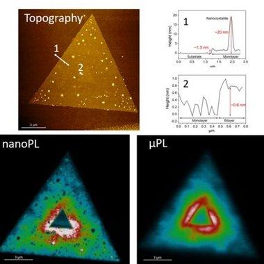
The flakes of monolayer tungsten disulfide (WS2) which is a direct‐gap semiconductor with an energy gap close to 2 eV and high photoluminescence quantum yield were analyzed with HORIBA LabRAM Nano using 532 nm p-polarized laser focused onto the cantilever-based silver coated TERS tip. Fig. 1 shows an AFM topographic image of a 14 µm triangular flake with 512 lines resolution as well as µPL and NanoPL (a.k.a. TEPL) maps acquired with a 500 ms integration time and pixel size of 93 nm. One can observe the higher resolution of the NanoPL image with respect to the µPL image:
(i) The contour of the triangular single crystalline flake as well as that of the thicker inner center triangle are much more well defined in the TEPL map than in the µPL image.
(ii) Dark spots of size ranging from 100 nm to 200 nm can clearly be seen in the TEPL map. They are likely to be nano-crystallites visible as bright features of few tens of nm of height.
(iii) The PL response non-uniformity on the outer monolayer part of the flake is resolved at the nanoscale, which reveals a lot of inhomogeneities. NanoPL reveals deep sub-diffraction limit details within the 2D WS2 flake that are not resolved in conventional µPL measurements [6, 7]. Edge effects, nanocrystallites, grain boundaries etc. are seen in the NanoPL image with improved signal to noise ratio and vastly improved resolution.
NanoRaman of WS2 exfoliated on template stripped silver
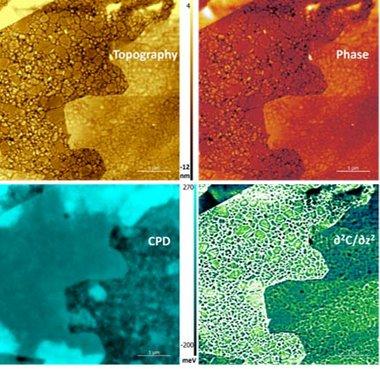
The understanding of charge transport and optimization of transistor mobility and current density in the fabrication of TMDCs based semiconductor devices requires study of semiconductor-insulator interfaces such as with SiO2/Si. Equally important is the interface between the semiconducting TMDC and the contact metal, as it is the locus of charge carrier injection and collection.In addition, it is key to correlate electronic characteristics with nanoscale excitonic and chemical properties provided respectively by TEPL and TERS measurements [8-11]. WS2 flakes exfoliated on template stripped silver have been characterized: 5.5 × 5.5 µm² images of topography, phase shift, contact potential difference (CPD, obtained with Kelvin probe measurement), and second derivative of capacitance (∂2C/∂z2) with 400 lines resolution, all obtained simultaneously with the AFM, are shown in Fig. 2. The surface potential (CPD) image shows significant inhomogeneities of both the silver substrate and the WS2 flake. Tip-Enhanced Raman (TERS) measurements are performed using a 638 nm p-polarized laser focused onto the vicinity of cantilever-based silver coated AFM-TERS tip.
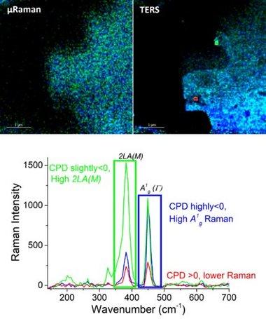
Two Raman maps are acquired in the same measurement in order to generate the µRaman and NanoRaman “at the same time”. The acquisition time of each spectrum is 150 ms and pixel size is 44 nm. Fig. 3 shows the µRaman and NanoRaman/TERS images generated from the integration of 418 cm-1 peak (in blue), and the 347 cm-1 peak (in green) corresponding to the A1g and 2LA(M) bands, respectively. The µRaman image with a diffraction-limited optical resolution features the flake but with blurred contours and a homogeneous distribution of both Raman signal intensities. In contrast, the higher resolution TERS image reveals much more details (Fig. 2):
(i) Much sharper edges of the flake
(ii) Inhomogeneities of the Raman signals, in particular of the A1g peak (in blue) with the presence of dark nanodomains.
There are apparent correlations between the features in CPD and TERS images (Fig. 2 and Fig. 3). This is clearly illustrated with average spectra taken from three different areas with positive CPD (~ 50 meV in red), negative CPD (~ -100 meV in green), highly negative CPD (~ -160 meV in blue) which exhibit low and equal 2LA (M) and A1g peaks, high 2LA (M), and high A1g peak, respectively. In the areas with lower CPD, locally formed metallic phases suppress the TERS response. These correlations between surface potential (CPD) and TERS signatures indicates the presence of inhomogeneities within interfacial electronic properties, which are attributed to variations in the local doping of the WS2 flakes[4].
NanoPL of WS2/WSxSe1-x/WSe2 heterostructure on SiO2/Si
Building up nanodevices from 2D layered materials requires heterostructures. The electrical and optical properties of such heterojunctions will depend on the alignment of the energy bands at the interface. Using alloys of transition metal dichalcogenides allows for band gap engineering which is likely to lead to sharp and well controlled interfaces. TEPL has already been applied to the MoSe2-WSe2 heterojunction for the study of quantum plasmonic injection and aging effect [12], here we present TEPL data obtained on a lateral single layer WS2/WSxSe1-x/WSe2 heterostructure grown on SiO2/Si.
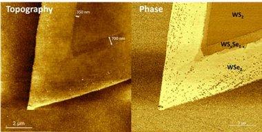
The 10×10 µm AFM topography and phase shift images (512 lines) show the apex of 60 µm triangular flake with a contrast allowing to distinguish the presence of both binary and the ternary alloys (Fig. 4). The nicely defined interfaces seen on both images allow the width of the ternary WSxSe1-x layer to be measured: 700 nm on one side of the flake apex and 350 nm on the other side.
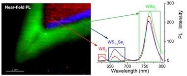
Tip-Enhanced Photoluminescence (TEPL) is performed with a 532 nm excitation laser and an AFM silver coated TERS tip. The acquisition time of each spectrum is 50 ms and pixel size is 100 nm. A three-color map (Fig. 5) including the TEPL response from WS2 (peak centered at 625 nm), WSxSe1-x (peak centered at 665 nm), WSe2 (peak centered at 765 nm) confirms the presence of the three single layer compounds as well as a difference in the WSxSe1-x PL signal quenched on the left side of the apex (appearing narrower on the height and phase shift images). The graph showing average spectra from the three regions indicates the integration PL response intervals (Fig. 5, right). The high spatial resolution obtained with the TEPL image reveals nanoscale information impossible to access with µRaman or µPL.
Conclusions
In this paper, we have presented new nano-imaging capabilities with correlated TERS, TEPL and AFM measurements of monolayer WS2 and WS2/WSxSe1-x/WSe2 heterojunction. Complementary morphological, chemical, and electronic structure information can be acquired simultaneously, with nanometer spatial resolution, with the HORIBA AFM-Raman systems.
We have demonstrated that TEPL, not limited by diffraction, provides a drastic improvement of the optical resolution compared to conventional Photoluminescence (µPL) and bring to light nanoscale heterogeneities impossible to access with conventional optical techniques. Single crystal WS2 flakes directly grown on SiO2/Si have been analyzed with TEPL: NanoPL response maps reveal variation in emission within a submicron size flake and nicely overlay on topography images (monolayer, bilayer, nanocrystallites). Beside these semiconductor/dielectric (SiO2) interfaces, results from probing TMCD/metal interfaces, namely WS2 on silver have been also shown. TERS and Kelvin probe measurements revealed nanoscale inhomogeneities both observed in CPD and Raman maps. Finally, NanoPL together with AFM topography data on a lateral single layer WS2/WSxSe1-x/WSe2 heterostructure grown on SiO2/Si have been presented and revealed nanoscale PL response variations beyond the smooth nano-resolution topography.
Acknowledgments
We thank the Nanoscopy team: We thank the contribution of Andrey Krayev and Ophélie Lancry for data collection, and Eddy Robinson for the manuscript correction. We thank Thomas Carlier for help in data processing. We thank all the R&D team (Alexey Belyayev, Dmitry Evplov, Vasily Gavrilyuk, Sergey Katsur, Alexander Yagovkin, Yury Turlapov, Maxim Eremin, Sergey Kostromin, Patrick Hsia, Philippe de Bettignies) for the development and support.
References
- W. Su et al, Nat Commun 9, 2891 (2018).
- K. K. H. Smithe et al, ACS Appl. Nano Mater., 1, 2, 572 (2018).
- T. P. Darlington et al, Nature Nanotechnology 15, 854 (2020).
- D. Moore et al, npj 2D Mater Appl 4, 44 (2020).
- T. Verhagen et al, ACS Appl. Nano Mater, 3, 7, 6563–6573 (2020).
- C. Kastl et al, 2D Mater. 4, 021024 (2017).
- Z. He et al, Sci. Adv. 5:eaau8763 (2019).
- Y. Okuno et al, Nanoscale 10, 14055 (2018).
- M. Rahaman et al, Nano Lett. 17 (10), 6027 (2017).
- Z. Zhang et al, Phys. Rev. B 97, 085305 (2018).
- C. Tang et al, Phys. Rev. B 98, 041402(R) (2018).
- P. K. Sahoo et al, Opt. Mater. Express 9, 1620 (2019).
Product & Exhibition information, Contact information
HORIBA AFM is designed to be combined with optical spectroscopies.
The HORIBA AFM platform allows fully-integrated use of confocal Raman microscopy and AFM for Tip-Enhanced Optical Spectroscopies (such as Tip-Enhanced Raman Spectroscopy (TERS) and Tip-Enhanced PhotoLuminescence (TEPL)), but also for truly co-localized AFM-Raman measurements. TERS and TEPL can provide nanoscale chemical and structural information, making the HORIBA AFM-Raman platform a two-way road, where complimentary techniques provide novel and unique imaging capabilities to each other. More information: AFM Optical Platform - HORIBA.
Masao Horiba Awards 2021 now accepting applications!
This year’s theme is ‘Optical/Spectroscopic Measurement Technologies for Life Science’
Upcoming Event (Plans to exhibit):EMRS Spring 31st May – 3rd June, XXVII ICORS 1st – 6th Aug (Rome), ICAVS 11 22nd – 27th Aug (Krakow), TERS 8 30th Aug - 1st Sept 2021 (Paris)
Upcoming e-Readout issues:Scanning NV magnetometry: surface magnetic fields at the nanoscale
e-Readout Editorial Office:
Research & Development Division, HORIBA, Ltd.
2, Miyanohigashi-cho, Kisshoin, Minami-ku, Kyoto 601-8510, Japan
E-mail : readout(at)horiba.co.jp

Agnès Tempez, PhD
AFM-Raman Application Scientist PP-TOFMS Product Manager HORIBA FRANCE SAS

Marc Chaigneau, PhD
Nanoscopy Director HORIBA FRANCE SAS
