We developed and demonstrated a new electron microanalysis technology, the internal-detector electron holography, which can visualize a 3D atomic structure image around a specific element using a widely-used scanning electron microscope (SEM) in lab-level, with Prof. Kouichi Hayashi (IMR, Tohoku Univ.) and Dr. Tomohiro Matsushita (JASRI). The internal-detector electron holography is a powerful and innovative technique for seeking and analyzing new materials or rare metals which is vital in the modern world of technology and science, since we can see clearly the smearing of light elements.
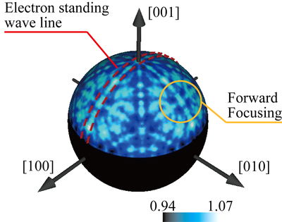
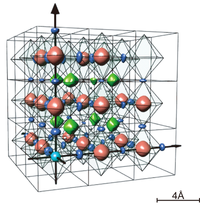
Until now, we have seen an atomic structure in only 2D image in the experiment. In order to progress to the next stage, Prof. Hayashi developed a new and innovative technology, the internal-detector electron holography based on an algorithm of the Atomic-Resolution Holography (*1), which has mainly been implemented in large experimental facilities, such as synchrotron radiation facilities, e.g. SPring-8. Using internal-detector electron holography, we can analyze the 3D atomic structure. In this research, the hologram (*2) shown in Fig.1 is measured from a standard sample (SrTiO3) and the atomic arrangement of is SrTiO3 shown in Fig.2 is clearly reconstructed with accuracy.
In the near future, this method should be applied to many fields, e.g. development of solar cells or catalysts since a 3D atomic arrangement can be reconstructed around a specific element with this method.
This work was supported by New Energy and Industrial Technology Development Organization (NEDO).
The result was published in Physical Review Letters (Online Publication, 21, July, 2011).
http://prl.aps.org/abstract/PRL/v107/i4/e045502
*1 Atomic-Resolution Holography
A reconstruction method of 3D atomic images around specific elements without prior knowledge of structures with electrons or X-rays whose wavelengths are A order.
*2 Hologram
A photograph recording the 3D information of the object by means of the nature of the waves. It is widely used in many fields, e.g. industry, medicine or many others. In our research, the measured pattern is called as "hologram" since it utilizes the wave feature.

Fig. 1
Holograms of SrTiO3. Two features, which are forward-focusing peaks and electron standing wave lines, can be observed.

Fig. 2
3D images of SrTiO3 reconstructed from the holograms. Green, red, and blue objects correspond to Sr, Ti, and O atoms, respectively.
Fig. 1 and Fig. 2 are cited from Phys. Rev. Lett. 107, 045502 (2011)